 | –≠–ª–µ–∫—Ç—Ä–æ–Ω–Ω—ã–π –∫–æ–º–ø–æ–Ω–µ–Ω—Ç: SPX2941U5 | –°–∫–∞—á–∞—Ç—å:  PDF PDF  ZIP ZIP |
1
Date: 08/25/04
SPX2941 1A Low Dropout Voltage Regulator
© Copyright 2004 Sipex Corporation
1A Low Dropout Voltage Regulator,
Adjustable Output, Fast Response
SPX2941
DESCRIPTION
FEATURES
Adjustable Output Down To 1.25V
Low Quiescent Current
Guaranteed 1.5A Peak Output Current
Low Dropout Voltage of 280mV @ 1A
Extremely Tight Load and Line
Regulation
Extremely Fast Transient Response
Reverse-battery Protection
Internal Thermal and Current Limit
Protection
Zero Current Shutdown
Error Flag Output for Out of Regulation
State
Standard TO-220 and TO-263
packages
Replacement for LM2941 and AS2941
Æ
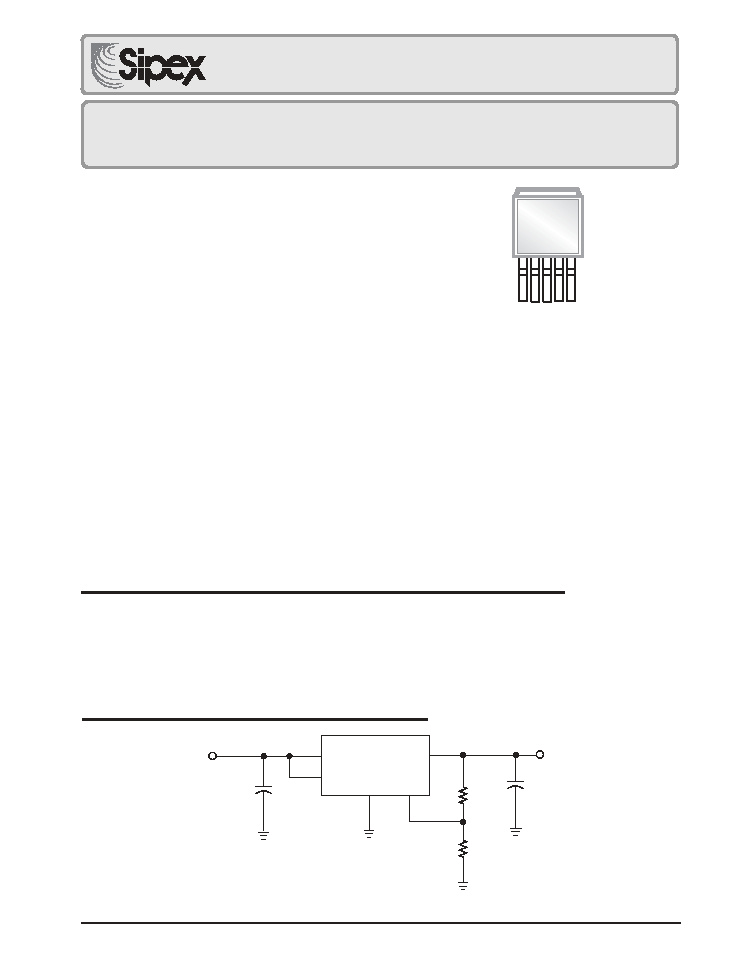
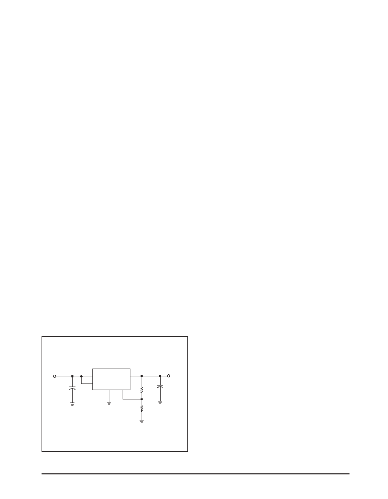
Figure 1. Adjustable Output Linear Regulator
The SPX2941 is a 1A, accurate voltage regulator with a low drop out voltage of 280mV(typ.) at
1A. These regulators are specifically designed for low voltage applications that require a low
dropout voltage and a fast transient response. They are fully fault protected against over-current,
reverse battery, and positive and negative voltage transients. Other features include Enable, and
Error Flag. The SPX2941 is offered in 5-pin TO-220 & TO-263 packages. For a 3A version, refer
to the SPX29300 data sheet.
SPX2941
V
OUT
V
IN
GND
ADJ
4
2
3
5
1
R1
R2
10µF
6.8µF
+
+
EN
TYPICAL APPLICATIONS CIRCUIT
Now Available in Lead Free Packaging
1 2 3 4 5
SPX2941
5 Pin TO-263
V
IN
GND
V
OUT
ADJUST
ENABLE
APPLICATIONS
Powering VGA & Sound Card
LCD Monitors
USB Power Supply
Power PC Supplies
SMPS Post-Regulator
High Efficiency Linear Power Supplies
Battery Charger
Portable Instrumentation
Constant Current Regulators
Adjustable Power Supplies
Date: 08/25/04
SPX2941 1A Low Dropout Voltage Regulator
© Copyright 2004 Sipex Corporation
2
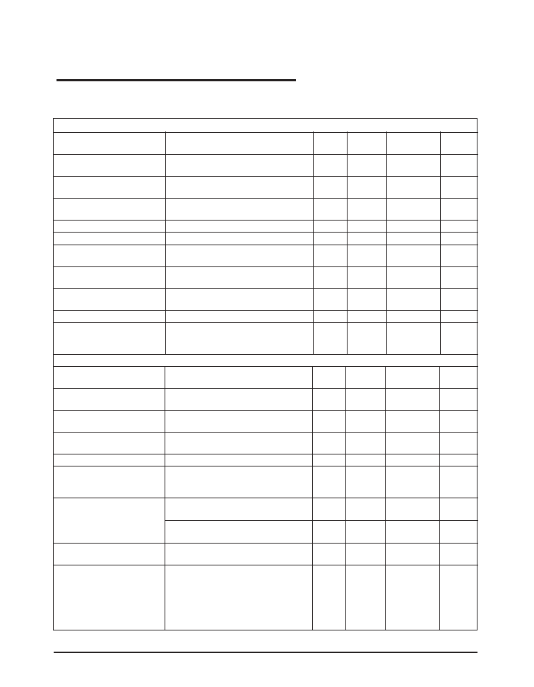
ABSOLUTE MAXIMUM RATINGS
Lead Temperature (soldering, 5 seconds) ................260∞C
Storage Temperature Range........................-65∞C to +150∞C
PARAMETER
CONDITIONS
MIN.
TYP.
MAX
UNIT
Reference Voltage
Adjustable version only
1.228
1.240
1.252
V
1.215
1.265
Adjust Pin Bias Current
40
80
V
120
Reference Voltage
(N
OTE
4)
20
ppm/∞C
Temperature Coefficient
Adjust Pin Bias Current
0.1
nA/∞C
Temperature Coefficient
Line Regulation
I
OUT
=10mA, (V
OUT
+1V)V
IN
16V
0.2
1.0
%
Load Regulation
V
IN
=V
OUT
+1V, 10mAI
OUT
I
FULL
0.3
1.5
%
Dropout Voltage (Note1)
I
OUT
=100mA
70
200
mV
(except 1.8V version)
I
OUT
=1A
280
550
Ground Current (Note3)
I
OUT
=750mA, V
IN
=V
OUT
+1V
12
25
mA
I
OUT
=1A
18
Ground Pin Current at
V
IN
=0.1V less than specified V
OUT
,
1.2
mA
Dropout
I
OUT
=10mA
Current Limit
V
OUT
=0V (Note2)
1.5
2.2
A
Output Noise Voltage
10Hz to 100kHz, I
OUT
=100mA,
C
L
=10µF
400
µV
RMS
C
L
=33µF
260
ERROR COMPARATOR (FLAG OUTPUT)
Output Leakage Current
V
OH
=16V
0.1
1
A
2
Output Low Voltage
Device set for 5V,
200
300
mV
V
IN
=4.5, I
OL
=250µA
400
Upper Threshold Voltage
Device set for 5V (Note 5)
40
60
mV
25
Lower Threshold Voltage
Device set for 5V (Note 5)
75
95
mV
140
Hysteresis
Device set for 5V (Note 5)
15
mV
Input Logic Voltage
LOW (OFF)
V
IN
<10V
0.8
V
HIGH (ON)
2.4
ENABLE Input Pin Current
V
EN
=16V
100
600
µA
750
V
EN
=0.8V
1
µ
A
2
Regulator Output Current
(N
OTE
6)
10
µA
in Shutdown
500
Thermal Resistance
TO-220
Junction to Case, at Tab
3
∞C/W
Junction to Ambient
60
TO-263
Junction to Case, at Tab
3
∞C/W
Junction to Ambient
60
V
IN
=V
OUT
+ 1V, I
OUT
=10mA, C
IN
=6.8
µF, C
OUT
=10
µF, T
A
= 25
∞C, unless otherwis specified. The boldface applies over the
junction temperature range. Adjustable versions are set at +5.0V.
Operating Junction Temperature Range......-40∞C to +125∞C
Input Supply Voltage (N
OTE
7) .... .....................................16V
ELECTRICAL CHARACTERISTICS
3
Date: 08/25/04
SPX2941 1A Low Dropout Voltage Regulator
© Copyright 2004 Sipex Corporation
N
OTE
1: Dropout voltage is defined as the input to output differential at which the output voltage drops to 99%
of its nominal value.
N
OTE
2: V
IN
=V
OUT(NOMINAL)
+1V; for example, V
IN
=4.3V for a 3.3V regulator. Employ pulse-testing procedures to
minimize temperature rise.
N
OTE
3: Ground pin current is the regulator quiescent current. The total current drawn from the source is the
sum of the load and ground currents.
N
OTE
4: Thermal regulation is defined as the change in the output voltage at a time T after a change in power
dissipation is applied, excluding load or line regulation effects.
N
OTE
5: Comparator threshold is expressed in terms of a voltage differential at the Adjust terminal below the
nominal reference voltage measured 6V input. To express these thresholds in terms of output
voltage change, multiply the error amplifier gain = V
OUT
/V
REF
= (R
1
+ R
2
)/R
2
. For example, at a
programmable output voltage of 5V, the Error output is guaranteed to go low when the output drops
by 95mVx 5V/ 1.240V = 38mV. Threshold remain constant as a percent of V
OUT
as V
OUT
is varied,
with the dropout warning occurring at typically 5% below nominal, 7.7% guaranteed.
N
OTE
6: V
EN
0.8V and V
IN
16V, V
OUT
= 0.
N
OTE
7: Maximum positive supply voltage of 20V must be of limited duration ( <100ms) and duty cycle (<1%).
The maximum continuous supply voltage is 16V.
N
OTE
8: V
REF
V
OUT
(V
IN
-1), 2.5V V
IN
16V, 10 mA I
C
I
FL
, T
J
< T
JMAX
.
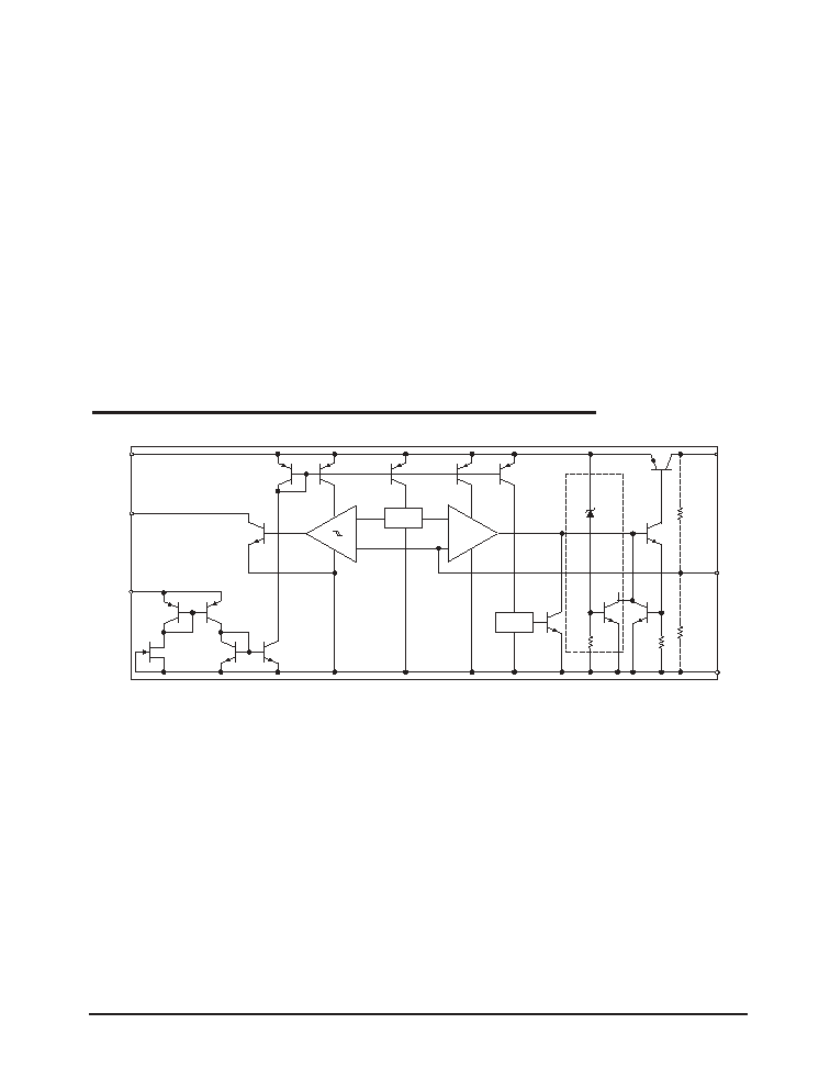
Reference
Thermal
Shutdown
EN
IN
OUT
ADJ
GND
O.V
I
LIMIT
28V
R1*
R2*
1.180V
1.240V +
+
-
-
FLAG
Figure 2. SP2941 Block Diagram
BLOCK DIAGRAM
Date: 08/25/04
SPX2941 1A Low Dropout Voltage Regulator
© Copyright 2004 Sipex Corporation
4
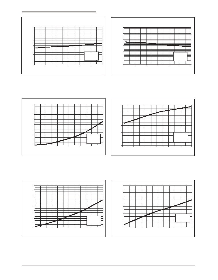
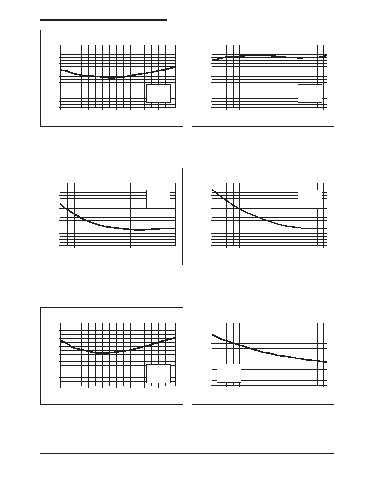
TYPICAL PERFORMANCE CHARACTERISTICS
Figure 3. Line Regulation for 3.3V Device
Figure 4. Load Regulation for 3.3V Device
Figure 7. Ground Current vs Load Current in Dropout
Figure 8. Dropout Voltage vs Load Current for 3.3V
Device
Figure 5. Ground Current vs Load Current for 3.3V Device Figure 6. Ground Current vs Input Current
3.320
3.315
3.310
3.305
3.300
3.295
3.290
3.285
3.280
4
6
8
10
12
14
16
V
IN
(V)
V
OUT
(V)
3.3V Device
IL = 10mA
CL = 10µF
3.310
3.305
3.300
3.295
3.290
3.285
3.280
IL (A)
V
OUT
(V)
0.00
0.25
0.50
0.75
1.00
1.25
1.50
3.3V Device
V
IN
= 4.3V
CL = 10µF
80.0
70.0
60.0
50.0
40.0
30.0
20.0
10.0
0.0
IL (A)
IGnd (mA)
0.00
0.25
0.50
0.75
1.00
1.25
1.50
3.3V Device
V
IN
= 4.3V
CL = 10µF
300
280
260
240
220
200
180
4
6
8
10
12
14
16
V
IN
(V)
IGnd (
µ
A)
3.3V Device
IL = 10mA
CL = 10µF
100
90
80
70
60
50
40
30
20
10
0
IL (A)
IGnd (mA)
0.00
0.25
0.50
0.75
1.00
1.25
1.50
3.3V Device
V
IN
= 3.2V
CL = 10µF
600
500
400
300
200
100
0
IL (A)
V
DR
OPOUT
(mV)
0.00
0.25
0.50
0.75
1.00
1.25
1.50
3.3V Device
CL = 10µF
5
Date: 08/25/04
SPX2941 1A Low Dropout Voltage Regulator
© Copyright 2004 Sipex Corporation
Figure 9. Ground Current vs Temperature at I
LOAD
=10mA
Figure 10. Output Voltage vs Temperature at I
LOAD
=10mA
Figure 11. Ground Current vs Temperature at I
LOAD
=500mA Figure 12. Ground Current vs Temperature in Dropout
at I
LOAD
=750mA
Figure 13. Ground Current vs Temperature at I
LOAD
=1.5A
Figure 14. Ground Current vs Temperature in Dropout at
I
LOAD
=1.5A
280
270
260
250
240
230
220
210
200
190
180
-40
-20
0
20
40
60
80
Temperature (∞C)
IGnd (
µ
A)
3.3V Device
V
IN
= 4.3V
IL = 10mA
CL = 10µF
120
100
3.320
3.310
3.300
3.290
3.280
3.270
3.260
3.250
3.240
3.230
3.220
-40
-20
0
20
40
60
80
Temperature (∞C)
V
OUT
(V)
3.3V Device
V
IN
= 4.3V
IL = 10mA
CL = 10µF
120
100
7.00
6.80
6.60
6.40
6.20
6.00
5.80
5.60
5.40
5.20
5.00
-40
-20
0
20
40
60
80
Temperature (∞C)
IGnd (mA)
3.3V Device
V
IN
= 4.3V
IL = 500mA
CL = 10µF
120
100
30
29
28
27
26
25
24
23
22
21
20
-40
-20
0
20
40
60
80
Temperature (∞C)
IGnd (mA)
3.3V Device
V
IN
= 3.2V
IL = 750mA
CL = 10µF
120
100
52.0
50.0
48.0
46.0
44.0
42.0
40.0
38.0
36.0
-40
-20
0
20
40
60
80
Temperature (∞C)
IGnd (mA)
3.3V Device
V
IN
= 4.3V
IL = 1.5A
CL = 10µF
120
100
100
95
90
85
80
75
70
-40
-20
0
20
40
60
80
Temperature (∞C)
IGnd (mA)
3.3V Device
V
IN
= 3.2V
IL = 1.5A
CL = 10µF
120
100
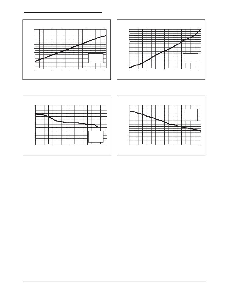
TYPICAL PERFORMANCE CHARACTERISTICS
Date: 08/25/04
SPX2941 1A Low Dropout Voltage Regulator
© Copyright 2004 Sipex Corporation
6
Figure 15. Dropout Voltage vs Temperature at I
LOAD
=750mA Figure 16. Dropout Voltage vs Temperature at I
LOAD
=1.5A
Figure 17. Enable Current vs Temperature for 3.3V Devices Figure 18. Enable Threshold vs Temperature for 3.3V
Devices
350
330
310
290
270
250
230
210
190
170
150
-40
-20
0
20
40
60
80
Temperature (∞C)
V
DR
OPOUT
(mV)
120
100
3.3V Device
IL = 750mA
CL = 10µF
500
480
460
440
420
400
380
360
340
320
-40
-20
0
20
40
60
80
Temperature (∞C)
V
DR
OPOUT
(mV)
120
100
3.3V Device
IL = 1.5A
CL = 10µF
35
30
25
20
15
10
5
0
-40
-20
0
20
40
60
80
Temperature (∞C)
I
EN
(
µ
A)
120
100
3.3V Device
V
IN
= 3.2V
IL = 750mA
CL = 10µF
2.00
1.90
1.80
1.70
1.60
1.50
1.40
1.30
1.20
1.10
1.00
-40
-20
0
20
40
60
80
Temperature (∞C)
V
TH
(V)
120
100
3.3V Device
V
IN
= 3.2V
IL = 750mA
CL = 10µF
TYPICAL PERFORMANCE CHARACTERISTICS
7
Date: 08/25/04
SPX2941 1A Low Dropout Voltage Regulator
© Copyright 2004 Sipex Corporation
APPLICATION INFORMATION
The SPX2941 incorporates protection against
over-current faults, reversed load insertion,
over temperature operation, and positive and
negative transient voltage.
Thermal Considerations
Although the SPX2941 offers limiting circuitry
for overload conditions, it is still necessary to
insure that the maximum junction tempera-
ture is not exceeded in the application. Heat
will flow through the lowest resistance path,
the junction-to-case path. In order to insure
the best thermal flow of the component, proper
mounting is required. Since the tab of the
device is electrically connected to GND, the
tab must be electrically isolated using a ther-
mally conductive spacer, which itself contrib-
utes some small additional thermal resistance.
Consult heatsink manufacturer for thermal
resistance and design of heatsink.
TO-220 Design Example:
Assume that V
IN
= 10V, V
OUT
= 5V, I
OUT
= 1A,
T
A
= 50∞C,
HA
= 1∞C/W,
CH
= 2∞C/W,
and
JC
= 3∞C/W, where
T
A
= ambient temperature,
HA
= heatsink to ambient thermal resistance,
CH
= case to heatsink thermal resistance,
JC
= junction to case thermal resistance.
The power calculated under these conditions
is:
P
D
= (V
IN
≠ V
OUT
) * I
OUT
= 5W,
and the junction temperature is calculated as
T
J
= T
A
+ P
D
* (
HA
+
CH
+
JC
) or
T
J
= 50 + 5.0 * (1 + 2 + 3) = 80∞C.
Reliable operation is insured.
Capacitor Requirements
The output capacitor is needed to insure
stability and minimize the output noise. The
value of the capacitor varies with the load.
However, a minimum value of 10µF alumi-
num capacitor will guarantee stability over all
load conditions. A tantalum capacitor is rec-
ommended if a faster load transient response
is needed.
If the power source has a high AC impedance,
a 0.1µF ceramic capacitor between input &
ground is recommended.
Minimum Load Current
To ensure a proper behavior of the regulator
under light load, a minimum load of 5mA for
SPX2941 is required.
Typical Application Circuit
Figure 18 shows a typical applications circuit
for an adjustable output regulator. The values
of R
1
and R
2
set the output voltage value as
follows: V
OUT
= V
REF
* [1 + (R
1
/R
2
)]. For best
results, the total series resistance should be
small enough to pass a minimum regulator
load current of 5 mA.
A minimum value of 10k is recommended
for R
2
with a range between 10k to 47k .
Figure 19. Adjustable Output Linear Regulator
SPX2941
V
OUT
V
IN
GND
ADJ
4
2
3
5
1
R1
R2
10µF
6.8µF
+
+
EN
Date: 08/25/04
SPX2941 1A Low Dropout Voltage Regulator
© Copyright 2004 Sipex Corporation
8
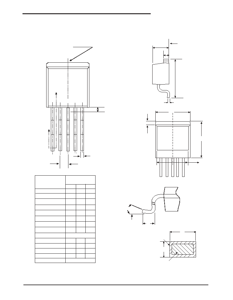
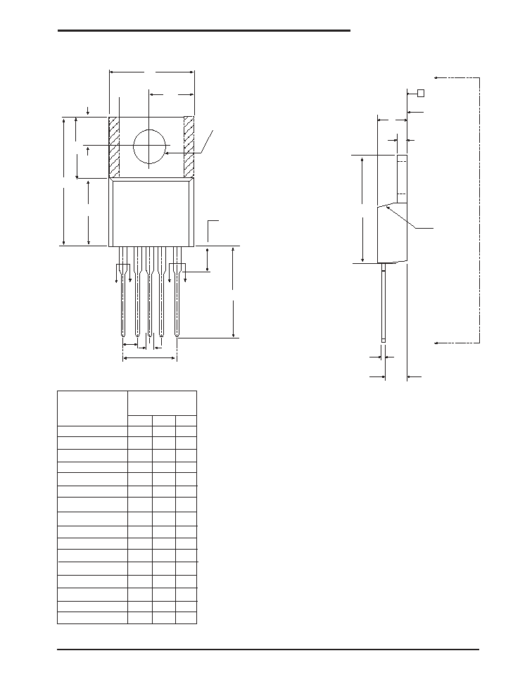
.160 - .190
0 - .010
Dimensions in (mm)
5 PIN TO-263
JEDEC TO-263
(BB) Variation
.020 - .039
.015 - .029
.070 - .110
-
- -
A
A1
b
c
E
E1
L
L1
L2
MIN NOM MAX
e
.067 BSC
.066
-
D1
.270 - -
.380 - .420
.245
-
-
H
.575 - .625
.070
L3
.010 BSC
c
WITH PLATING
BASE METAL
(b)
CONTACT AREA
1
2
3
4
5
E
E
L2
5X b
e
4X
(DATUM A)
c2
.045 - .023
c
C2
A
H
SEATING PLANE
D1
L1
(E)
E1
L
0∫-8∫
L3
5 PIN TO-263
PACKAGE: 5PIN TO-263
9
Date: 08/25/04
SPX2941 1A Low Dropout Voltage Regulator
© Copyright 2004 Sipex Corporation
.160 - .190
Dimensions in
(inches)
5 PIN TO-220
.015 - .040
A
b
C1
D
E
MIN NOM MAX
e
e1
F
H1
J1
P
Q
U
V
L
.014 - .022
.560 - .590
.385 - .415
.385 - .415
.062 - .072
.045 - .055
.234 - .258
.090 - .115
.540 - .560
.146 - .156
.103 - .113
- .30 -
- .24 -
L1
- .250
D
B
SEATING
PLANE
F
A
CHAMFER
OPTIONAL
C1
J1
A
A
E
¯P
Q
D
D1
E/2
L
L1
C C
D
D
b
e1
H1
e
5 PIN TO-220
PACKAGE: 5PIN TO-220

Date: 08/25/04
SPX2941 1A Low Dropout Voltage Regulator
© Copyright 2004 Sipex Corporation
10
Corporation
ANALOG EXCELLENCE
Sipex Corporation reserves the right to make changes to any products described herein. Sipex does not assume any liability arising out of the
application or use of any product or circuit described herein; neither does it convey any license under its patent rights nor the rights of others.
Sipex Corporation
Headquarters and
Sales Office
233 South Hillview Drive
Milpitas, CA 95035
TEL: (408) 934-7500
FAX: (408) 935-7600
PART NUMBER .................... ACCURACY ... OUTPUT VOLTAGE ...................... PACKAGE
SPX2941T5 ............................ 3% ........................ Adj ............................. 5 lead TO-263
SPX2941T5/TR ...................... 3% ........................ Adj ............................. 5 lead TO-263
SPX2941U5 ........................... 3% ........................ Adj ............................. 5 lead TO-220
PACKAGE PINOUTS
ORDERING INFORMATION
TO-263-5 Package (T5)
Top View
4 5
3
2
1
TO-220-5 Package (U5)
Top View
1 2 3 4 5
V
IN
GND
V
OUT
1)
3)
4)
5)
2) Enable
ADJUST
SPX2941
Available in lead free packaging.To order add "-L" suffix to part number.
Example: SPX2941T5/TR = standard; SPX2941T5-L/TR = lead free
/TR = Tape and Reel
Pack quantity is 500 for TO-263.